RT1719 Application Note: Implementation and Safe Use of USB PD Protocols in Sink Systems
Will Lin | AN074
The RT1719 is a USB Type-C controller that complies with the latest USB Type-C and Power Delivery (PD) standards. The RT1719 manages tasks related to USB Type-C detection, including attachment and orientation. The RT1719 integrates the physical layer of the USB BMC power delivery protocol, enabling power delivery up to 100W. The BMC PD block fully supports the Type-C specification. This application note will introduce the most prevalent uses and applications of the RT1719.
1 Sink PDO Setting Framework
Generally, the system in use consumes power from the Type-C port which RT1719 controls. It is recommended to configure Table_SEL, PSEL2, and PSEL1 as the power for full functionality operation.
If the sink system intends to check the source capabilities and to operate according to the given source power, the recommended settings and flow are provided as follows.
1. MCU can be powered up when VBUS = 5V.
2. Set Table_SEL, PSEL2, and PSEL1 as the power for full function operation.
3. Set the Path_Opt as 001b.
For a more detailed understanding of the control flow, please refer to the subsequent sections. For instance, you can find more information about the "Mismatch block" in the Mismatch section. The process of checking is elaborated in the Check Source Ability section, and the procedure for Requesting the other PDO is discussed in the Source PDO Selection by MCU section.
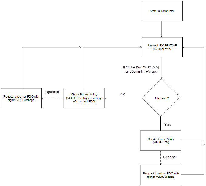
Figure 1. MCU Control Flow
1.1 Sink PDO Configuration and
Path_Opt
Table_SEL
There are 128 Sink_Capabilities that can be configured. 64 Sink_Capabilities are in Table 1. The sink currents of each Sink PDO in the Sink capability are the same. The other 64 Sink_Capabilities are in Table 0. The sink powers of each Sink PDO in the Sink capability are the same, except for the one of which the sink current is over 5A.
Table 1. Table_SEL Setting
|
Table Setting
|
Configure in Pin 18
|
0x3C[6]
|
|
Table 1
|
10kΩ to VCAP (pin 10)
|
1b
|
|
Table 0
|
10kΩ to GND
|
0b
|
PSEL
PSEL2 (pin 3) and PSEL1 (pin 4) are capable of configuring 64 settings. The sink capability can be configured according to Table select, PSEL2, and PSEL1.
Table 2. PSEL2 Setting
|
PSEL2 Setting
|
Resistance between PSEL2 and GND
(unit: kΩ) (±1%)
|
0x3C[5:3]
|
|
111
|
Open
|
111b
|
|
110
|
887
|
110b
|
|
101
|
649
|
101b
|
|
100
|
453
|
100b
|
|
011
|
324
|
011b
|
|
010
|
143
|
010b
|
|
001
|
56.2
|
001b
|
|
000
|
0
|
000b
|
Table 3. PSEL1 Setting
|
PSEL1 Setting
|
Resistance between PSEL1 and GND
(unit: kΩ) (±1%)
|
0x3C[2:0]
|
|
111
|
Open
|
111b
|
|
110
|
887
|
110b
|
|
101
|
649
|
101b
|
|
100
|
453
|
100b
|
|
011
|
324
|
011b
|
|
010
|
143
|
010b
|
|
001
|
56.2
|
001b
|
|
000
|
0
|
000b
|
Path_Opt
Table 4. Path_Opt Setting
|
Path Option Setting
|
Resistance between Path_Opt and GND
(unit: kΩ) (±1%)
|
0x3F[2:0]
|
Behavior
|
HV Bound
|
LV Bound
|
|
Option 7
|
Open
|
111b
|
The same with Path option = 000
|
The same with Path option 0
|
The same with Path option 0
|
|
Option 6
|
887
|
110b
|
PATHEN is low no matter if Sink PDO is matched with Source PDO.
|
20V
|
5V
|
|
Option 5
|
649
|
101b
|
PATHEN is low no matter if Sink PDO is matched with Source PDO.
|
15V
|
5V
|
|
Option 4
|
453
|
100b
|
PATHEN is low no matter if Sink PDO is matched with Source PDO.
|
12V
|
5V
|
|
Option 3
|
324
|
011b
|
PATHEN is low no matter if Sink PDO is matched with Source PDO.
|
9V
|
5V
|
|
Option 2
|
143
|
010b
|
PATHEN is low no matter if Sink PDO is matched with Source PDO.
|
5V
|
5V
|
|
Option 1
|
56.2
|
001b
|
PATHEN is low no matter if Sink PDO is matched with Source PDO.
|
Depending on Max. V of the Sink capability.
|
1. Match: Depending on the requested PDO.
2. Mismatch: 5V
|
|
Option 0
|
0
|
000b
|
1. Match: PATHEN is low.
2. Mismatch: PATHEN is high.
|
Depending on Max. V of the Sink capability.
|
1. Match: Depending on the requested PDO.
2. Mismatch: 5V
|
1.2
I2C
Address
The RT1719 can be configured to four slave addresses by setting the resistance between ADDR (pin 12) and GND.
Table 5. RT1719 I2C Address Setting
|
I2C Address in 7bit
|
Resistance between ADDR and GND (unit: kΩ) (±1%)
|
|
0x40
|
0
|
|
0x41
|
309
|
|
0x42
|
649
|
|
0x43
|
Open
|
The I2C interface bus must be connected to the power node using a resistor of 1kΩ, and it should have an independent and separate connection to the processor.
1.3
Mismatch
There are four results for each attachment or receiving Source_Capabilities.
Table 6. Mismatch Indication
|
SPDO_MIS
(0x10[3])
|
TYPEC_MIS
(0x0F[0])
|
VBUSONLY_MIS
(0x0E[3])
|
Note
|
|
0
|
0
|
0
|
There is at least one condition (PD, Type C only, or VBUS only) matching with Table_SEL, PSEL settings.
|
|
0
|
0
|
1
|
The source device does not have PD ability and there is no Rp at CC pin.
The source ability (5V, 500mA) is mismatched with Table_SEL, PSEL settings.
|
|
0
|
1
|
0
|
The source device is a Type-C-only device.
The source ability advertised by Rp is mismatched with Table_SEL, PSEL settings.
|
|
1
|
0
|
0
|
The source device is a PD device.
The Source PDO in Source_Capabilities are mismatched with Table_SEL, PSEL settings.
|
1.4
Check
the Source Ability
The Source indicates its capabilities through the Source Capability (recorded in 0x11 to 0x2C) or the Rp level (0x38[3:0]). The Source Capability takes higher priority than the Rp level. It is recommended to check the source ability according to the flows shown in Figure 2.
Please refer to the Read Source PDO section for reading source PDO.
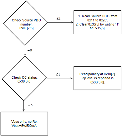
Figure 2. Flow for Source Ability Flow
1.5
Check
CC Status
The RT1719 is able to report the CC status. According to the information reported, the system can obtain attach orientation and Rp level. The source ability is based on the Rp level in Type-C stage or with Type-C-Only Source attached. The orientation can also be checked in 0x10[7].
Table 7. CC Status
|
|
CC1 (0x38[1:0])
|
|
00
|
01
|
10
|
11
|
|
CC2 (0x38[3:2])
|
00
|
Open
|
Attached at CC1.
Source is 5V, 0.5A.
|
Attached at CC1.
Source is 5V, 1.5A.
|
Attached at CC1.
Source is 5V, 3A.
|
|
01
|
Attached at CC2.
Source is 5V, 0.5A.
|
Debug ACC
|
Debug ACC
|
Debug ACC
|
|
10
|
Attached at CC2.
Source is 5V, 1.5A.
|
Debug ACC
|
Debug ACC
|
Debug ACC
|
|
11
|
Attached at CC2.
Source is 5V, 3A.
|
Debug ACC
|
Debug ACC
|
Debug ACC
|
1.6
Read
Source PDO
The RT1719 can record the source cap in the register from 0x11 to 0x2C. There is one Source PDO with Vbus = 5V at least and seven Source PDOs at most in the Source Capability. Register 0x0F[7:5] shows how many Source PDOs are in the Source Capability.
Please note that RT1719 will only compare the Fixed supply of Source PDO with Sink PDO.
The selected Source PDO is recorded in register 0x10[2:0].
Table 8. Source PDO Registers
|
PDO
|
Information
|
Register
|
Description
|
|
1st PDO
|
Power Type
|
0x14[7:6]
|
00b: Fixed supply
01b: Battery supply
10b: Variable supply
11b: Programmable Power supply
|
|
Vbus Voltage
|
0x13[3:0] (MSB) and 0x12[7:2] (LSB)
|
Unit: 50mV
|
|
Current
|
0x12[1:0] (MSB) and 0x11[7:0] (LSB)
|
Unit: 10mA
|
|
2nd PDO
|
Power Type
|
0x18[7:6]
|
00b: Fixed supply
01b: Battery supply
10b: Variable supply
11b: Programmable Power supply
|
|
Vbus Voltage
|
0x17[3:0] (MSB) and 0x16[7:2] (LSB)
|
Unit: 50mV
|
|
Current
|
0x16[1:0] (MSB) and 0x15[7:0] (LSB)
|
Unit: 10mA
|
|
3rd PDO
|
Power Type
|
0x1C[7:6]
|
00b: Fixed supply
01b: Battery supply
10b: Variable supply
11b: Programmable Power supply
|
|
Vbus Voltage
|
0x1B[3:0] (MSB) and 0x1A[7:2] (LSB)
|
Unit: 50mV
|
|
Current
|
0x1A[1:0] (MSB) and 0x19[7:0] (LSB)
|
Unit: 10mA
|
|
4th PDO
|
Power Type
|
0x20[7:6]
|
00b: Fixed supply
01b: Battery supply
10b: Variable supply
11b: Programmable Power supply
|
|
Vbus Voltage
|
0x1F[3:0] (MSB) and 0x1E[7:2] (LSB)
|
Unit: 50mV
|
|
Current
|
0x1E[1:0] (MSB) and 0x1D[7:0] (LSB)
|
Unit: 10mA
|
|
5th PDO
|
Power Type
|
0x24[7:6]
|
00b: Fixed supply
01b: Battery supply
10b: Variable supply
11b: Programmable Power supply
|
|
Vbus Voltage
|
0x23[3:0] (MSB) and 0x22[7:2] (LSB)
|
Unit: 50mV
|
|
Current
|
0x22[1:0] (MSB) and 0x21[7:0] (LSB)
|
Unit: 10mA
|
|
6th PDO
|
Power Type
|
0x28[7:6]
|
00b: Fixed supply
01b: Battery supply
10b: Variable supply
11b: Programmable Power supply
|
|
Vbus Voltage
|
0x27[3:0] (MSB) and 0x26[7:2] (LSB)
|
Unit: 50mV
|
|
Current
|
0x26[1:0] (MSB) and 0x25[7:0] (LSB)
|
Unit: 10mA
|
|
7th PDO
|
Power Type
|
0x2C[7:6]
|
00b: Fixed supply
01b: Battery supply
10b: Variable supply
11b: Programmable Power supply
|
|
Vbus Voltage
|
0x2B[3:0] (MSB) and 0x2A[7:2] (LSB)
|
Unit: 50mV
|
|
Current
|
0x2A[1:0] (MSB) and 0x29[7:0] (LSB)
|
Unit: 10mA
|
1.7
Source
PDO Selection by MCU
After reading Source Capability, the system master can request another source PDO through I2C. Please refer to the following steps:
1. Set the evaluation mode as evaluating per register setting by 0x03[4] = 1b.
2. Set the PDO number in 0x03[2:0].
3. Initiate a Request for the source PDO by setting 0x04[7] = 1b.
Please note that setting 0x03[2:0] = 000b or other invalid values (such as 0x03[2:0] = 110b but there are only five source PDOs) will trigger an I2C error (0x36[0] = 1b). Please do not set Path_Opt as 000 or 111 if MCU intends to select the Source PDO.
After initiating the Request successfully, there will be three results as reported in 0x34[3:1]. If Source sends PS_RDY, IRQB will be low due to 0x35[2]. After receiving PS_RDY, the sink system can start to sink.
Please refer to Figure 3 for a more detailed flow.
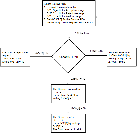
Figure 3. MCU Selecting Source PDO Flow
In addition to responding to the message, the sink capability will be modified. If the system master requests the first PDO (5V), the sink capability will be updated to 5V (with the current set according to the 5V Source PDO).
If the system master requests another valid PDO (9V, for example), the sink capability will be modified to 5V (with current set according to Table_SEL, PSEL2 and PSLE1) and 9V (with the current set according to the 9V Source PDO).
Table 9 shows the updated results of related registers.
Table 9. Sink PDO Change After MCU Selecting Source PDO
|
MCU Selection
|
MCU Select Current
0x73[1:0] (MSB) and 0x72 (LSB)
|
MCU Select Voltage
0x75[1:0] (MSB) and 0x74 (LSB)
|
5V Current
0x77[1:0] (MSB) and 0x76 (LSB)
|
Currents of other PDO
0x79[1:0] (MSB) and 0x78 (LSB)
0x7B[1:0] (MSB) and 0x7A (LSB)
0x7D[1:0] (MSB) and 0x7C (LSB)
0x7F[1:0] (MSB) and 0x7E (LSB)
|
|
The 1st PDO
|
According to the requested Source PDO
|
5V
|
According to the requested Source PDO
|
0A
|
|
Another valid PDO
|
According to the requested Source PDO
|
According to the requested Source PDO
|
According to Table_SEL, PSEL2 and PSEL1
|
0A
|
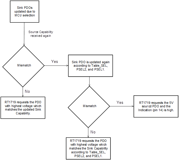
Figure 4. RT1719 Sink PDO Change Rule
2
Sink
Path Setting
Soft-Start is necessary for sink path if the capacitance of the Sink system is high. The higher the capacitance, the more serious the thermal stress on the sink path MOSFET.
It is recommended to parallel two or more MOSFETs to share the thermal stress. The high SOA performance MOSFET is also recommended.
The MOSFET selection for SOA is detailed in Table 10.
Table 10. Suggested SOA of VBUS Path PMOS Suggestion
|
VBUS\C1
|
47 (µF)
|
100 (µF)
|
220 (µF)
|
330 (µF)
|
440 (µF)
|
|
5V
|
SOA:
VDS = 5V
Pulse = 10ms
Id = 0.025A
|
SOA:
VDS = 5V
Pulse = 10ms
Id = 0.05A
|
SOA:
VDS = 5V
Pulse = 10ms
Id = 0.075A
|
SOA:
VDS = 5V
Pulse = 10ms
Id = 0.1A
|
SOA:
VDS = 5V
Pulse = 10ms
Id = 0.2A
|
|
9V
|
SOA:
VDS = 9V
Pulse = 10ms
Id = 0.2A
|
SOA:
VDS = 9V
Pulse = 10ms
Id = 0.3A
|
SOA:
VDS = 9V
Pulse = 10ms
Id = 0.5A
|
SOA:
VDS = 9V
Pulse = 10ms
Id = 0.8A
|
SOA:
VDS = 9V
Pulse = 10ms
Id = 1A
|
|
12V
|
SOA:
VDS = 20V
Pulse = 10ms
Id = 0.2A
|
SOA:
VDS = 20V
Pulse = 10ms
Id = 0.6A
|
SOA:
VDS = 20V
Pulse = 10ms
Id = 0.8A
|
SOA:
VDS = 20V
Pulse = 10ms
Id = 1.2A
|
SOA:
VDS = 20V
Pulse = 10ms
Id = 1.6A
|
|
15V
|
SOA:
VDS = 20V
Pulse = 10ms
Id = 0.5A
|
SOA:
VDS = 20V
Pulse = 10ms
Id = 0.75A
|
SOA:
VDS = 20V
Pulse = 10ms
Id = 1.2A
|
SOA:
VDS = 20V
Pulse = 10ms
Id = 1.6A
|
SOA:
VDS = 20V
Pulse = 10ms
Id = 2A
|
|
20V
|
SOA:
VDS = 20V
Pulse = 10ms
Id = 0.5A
|
SOA:
VDS = 20V
Pulse = 10ms
Id = 1A
|
SOA:
VDS = 20V
Pulse = 10ms
Id = 1.75A
|
SOA:
VDS = 20V
Pulse = 10ms
Id = 2.5A
|
SOA:
VDS = 20V
Pulse = 10ms
Id = 3A
|
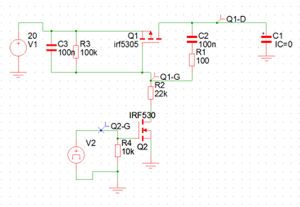
Figure 5. Simulation Circuit for Soft-Start of VBUS Sink Path
3
Conclusion
In conclusion, the sink system with a MCU can adapt its operation based on the capabilities of the source. This approach enhances safety for various applications. The information provided in this application note simplifies the implementation of the checking flow. Furthermore, it explains how the system master can request different PDOs and how these requests affect the sink capability. The note also provides guidance on handling I2C interface and interpreting the outcomes of the request initiation. This information facilitates effective and safe use of USB PD protocols.
The above concludes all the contents covered in this application note. To stay updated with more information about our products, please subscribe to our newsletter.